
Electron Microscopes


Ted Pella Inc COPPER TAPE COND.SGL ADH.

Copper Conductive Tape, 6.3mm W x 16.4m L; 1/4 in. x 18yd, Core diameter is 76mm, Foil Thickness: 0.04mm, Total Thickness: 0.07mm, Resistance through Adhesive: 0.005ohm


Electron Microscopy Sciences Shorter Pin SEM Stub Slotted 1/2" Head with Shorter Pin (6 mm), Aluminum, 1/8" Pin diameter
Cambridge, Phillips, Camscan, B&L, Etec, Zeiss SEM specimen mounts. Tapered end pin, slotted head.
Head: 1/2"
Pin height: 6 mm
Pin diameter: 1/8"


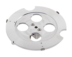
Electron Microscopy Sciences SEM Pin Stub Holder for 12 Zeiss 12.7 mm
This 62 mm in diameter multi pin holder is designed to save time. It is made from machined aluminum with stainless steel Allen wrench screws. It accommodates up to twelve standard 12.7 mm (1/2") pin stubs
Type: Zeiss with Built-in Dovetail
Med Vet International Trocar-Trocar I. M. Pin, 7/64" x 8", J0250D
Highest quality type 316L stainless steel IM pins. Available in the points and diameters listed below. When ordering, please match diameter with point style number. Made in U.S.A.
Electron Microscopy Sciences Pikal Care
A thinner paste for use on stainless steel and surfaces. Can be applied with a wipe or directly to the surface.
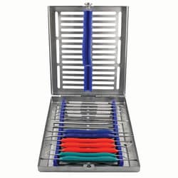
Med Vet International Dental Probes/Picks Sterilization Cassettes - 15 Probes/Scalers, J1510A, Each
Can hold 15 probes and scalers. Actual product dimensions: 7.4" (18.5cm) x 8" (20cm) x 1.77" (4.5cm)
Electron Microscopy Sciences SEM Wafer Holder, 100 mm
These wafer holders are made from aluminum and feature brass clips which secure the wafers. Each holder comes with a 0.125" (3.2 mm) pin of 0.375" (9.5 mm) length. Accomodates 4" (100 mm) diameter wafer.
Size: 100 mm

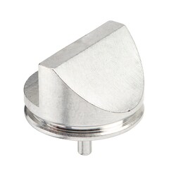
Electron Microscopy Sciences Standard Pin SEM Stub 70° Low Profile, 1/2" Head with 3/8" Pin, Aluminum
70° low profile SEM specimen mount for use with FEI, Tescan, Zeiss, Philips, LEO, Cambridge, AMRAY, Leica, CamScan, ETEC. Made from ultra-pure aluminum.
Head: 1/2"
Pin height: 3/8"

Electron Microscopy Sciences Shorter Pin Mini SEM Stub Mini Pin Stub with Short Pin, Stainless
Mini SEM stub specimen mount with shorter pin (6 mm) for use with all Zeiss/LEO scanning electron microscopes, FE-SEMs & FIB systems. Made of stainless steel.
Head: 6.6 x 1.3 mm
Pin height: 6.25 mm
Electron Microscopy Sciences Standard Pin SEM Stub Combo 45-90°, 1" Head with 3/8" Pin, Aluminum
45°/90° SEM specimen mount with aluminum slotted head for use with FEI, Tescan, Zeiss, Philips, LEO, Cambridge, AMRAY, Leica, CamScan, ETEC. Made from ultra-pure aluminum.
Head: 1"
Pin height: 3/8"